
Getting Started with PCB Design: A Beginner's Complete Guide
Everything a beginner needs to know — from schematic capture to generating your first Gerber files ready for manufacturing.
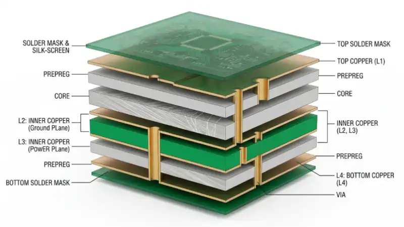
Understanding PCB Layer Stack-Up: 2, 4 and 6 Layers Explained
How to choose the right number of copper layers for your project — and why it matters for signal integrity and cost.

Top 5 Free PCB Design Tools for Students and Makers
KiCad, EasyEDA, Fritzing and more — a practical guide to the best free EDA tools that won't cost you a rupee.

How to Read and Verify Gerber Files Before Sending to Manufacture
A step-by-step walkthrough for inspecting your Gerber output before it reaches the fab — catch errors before they become costly mistakes.

PCB Trace Width Guide: Sizing Copper Tracks for Your Current Requirements
How wide does your trace actually need to be? Learn the IPC-2221 formula, common rules of thumb and practical examples for everyday designs.
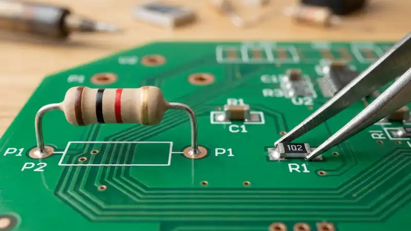
SMD vs Through-Hole: Which Component Package Is Right for Your Project?
SMD components are smaller and cheaper at scale; through-hole parts are easier to solder by hand. Here's how to decide — and when to mix both.
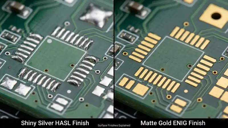
PCB Surface Finishes Explained: HASL, ENIG, OSP and More
Solder mask, silkscreen and surface finish affect solderability, durability and cost. This guide explains every option so you can pick the right one.
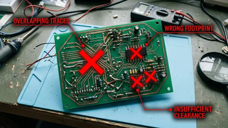
10 Common PCB Design Mistakes Beginners Make (and How to Avoid Them)
From wrong footprints to missing decoupling caps — the errors that appear most often in student and maker projects, and exactly how to fix them.

Designing a 4-Layer PCB: Power Planes, Signal Routing and EMI Control
When a 2-layer board is no longer enough, a 4-layer stackup unlocks dedicated power planes and dramatically cleaner routing. Here's how to set one up.
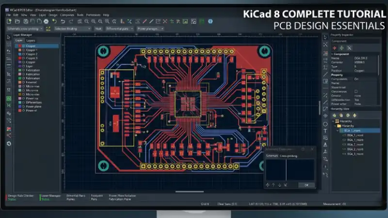
KiCad 8 Complete Tutorial: From Schematic to Gerber in One Session
A hands-on walkthrough of KiCad 8 — install the app, draw a schematic, assign footprints, lay out the board and export Gerbers ready for PCB LAB.