Every PCB designer has received a board back from the fab only to discover an embarrassing error they could have caught with one more look. Here are the ten mistakes that appear most often in student and first-time maker designs — and exactly how to prevent each one.
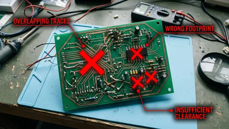
1. Wrong Footprint Size
What happens: The component arrives and its pads don't align with the board's pads. Best case: you bodge it with bent leads. Worst case: you have to order a respin.
Fix: Always verify the footprint against the component datasheet's recommended land pattern — not just the package name. Print the footprint at 1:1 scale and physically place the component on paper to confirm the fit before ordering.
2. Missing Decoupling Capacitors
What happens: The circuit works on a breadboard but is unstable on the PCB — random resets, logic errors, noise on the power rail.
Fix: Place a 100 nF ceramic capacitor as close as possible to every IC power pin (VCC, VDD, AVCC). For high-current ICs, add a 10 µF bulk capacitor nearby too. This is non-negotiable for any digital circuit.
3. Power Traces Too Narrow
What happens: The trace heats up, voltage droops and components behave erratically or fail entirely.
Fix: Use our trace width guide to size power traces correctly. As a quick rule: never go below 0.5 mm for any trace carrying more than 500 mA.
4. Poor or Missing Ground Plane
What happens: High-frequency noise couples into sensitive circuits, ground bounce causes glitches, EMI emissions are elevated.
Fix: Add a copper pour tied to GND on the bottom copper layer. In KiCad: Add Zone → select B.Cu → assign net GND → fill. Ensure all GND pins connect to the pour with short vias.
5. Skipping the DRC
What happens: Traces that are too close together, pads outside the board outline or unconnected nets make it to the fab — and your boards come back broken.
Fix: Run the Design Rule Check (DRC) in your EDA tool before every Gerber export. Fix every error; review every warning. Make this a mandatory last step.
6. Unlabelled Connectors
What happens: You receive the board, look at the three identical 2-pin connectors and have no idea which one is power and which one is UART.
Fix: Label every connector on the silkscreen with its function and pin assignment (e.g., "J1 — VIN / GND" or "UART: TX / RX / GND / VCC"). This takes five minutes in the schematic and saves hours of confusion during assembly.
7. 90-Degree Trace Bends
What happens: For RF and high-speed signals, sharp corners create impedance discontinuities and antenna-like structures. For standard fab processes, the acid can pool in corners and under-etch them.
Fix: Route all bends at 45 degrees, or use curved arcs. Most EDA routers do this automatically when configured correctly (KiCad: interactive router mode uses 45-degree bends by default).
8. Drill Size Below Fab Minimum
What happens: The fab cannot drill the hole and either rejects the file or substitutes the nearest available drill size — which may not fit your component.
Fix: PCB LAB minimum finished hole diameter is 0.3 mm. Check all vias and through-hole pads before exporting. In KiCad, set the DRC rule to enforce this minimum automatically.
9. Pads Too Small for Hand Soldering
What happens: You receive perfectly manufactured boards but cannot solder them because the pads are the same size as the IC lands with no room for an iron tip.
Fix: For hand-soldering, use footprints with extended pads — add 0.5 mm to each end of SMD pads. Many KiCad footprint libraries include dedicated "hand-soldering" variants. Avoid 0402 packages until you are comfortable with 0603 and 0805.
10. Copper Too Close to the Board Edge
What happens: The routing or panelisation process breaks out the board and nicks the copper trace, causing an open circuit right at the edge.
Fix: Maintain at least 0.3 mm clearance between any copper feature and the board outline. PCB LAB recommends 0.5 mm for safety margin. Set this as a DRC constraint in your EDA tool and you will never violate it.
The single most effective habit: after routing, zoom to 1:1 on screen, toggle each layer on and off, and visually walk the entire board before running DRC. Your eyes catch errors that automated tools sometimes miss.
Checked all 10? Let's build it.
5 boards — ₹450 total (₹150 setup + ₹300)
10 boards — ₹750 total (₹150 setup + ₹600) | Max 2 orders / month
Get a Quote →