When you look at a finished PCB you see three surface layers on top of the copper: the solder mask (that distinctive green — or red, or blue — coating), the silkscreen (the white component labels), and the surface finish on the exposed copper pads. Each one has options, and your choices affect cost, shelf life and how well the board solders.
Solder Mask
Solder mask is a polymer coating applied over the copper layers. It does two things: protects the copper from oxidation and prevents solder bridges between adjacent pads during assembly.
Colour options: Green is the most common — and cheapest — because it is the standard photolithography chemistry that fabs have optimised over decades. Other options include blue, red, black, white and yellow. They look great but add a small cost premium. For a first prototype, green is the practical choice.
Openings in the solder mask (where copper is exposed for soldering) are defined by your Gerber solder mask layers. The gap between a pad edge and the mask edge is the solder mask expansion — PCB LAB default is 0.05 mm per side.
Silkscreen
Silkscreen (also called legend or overlay) is a layer of ink printed on top of the solder mask. It carries:
- Component reference designators (R1, C4, U2…)
- Polarity marks (+ for capacitors, pin-1 dots or notches for ICs)
- Board name, version number and any regulatory marks
- Connector labels (UART, GND, VCC…)
White on green is standard. Always confirm that silkscreen text is above the fab's minimum stroke width — PCB LAB requires at least 0.15 mm stroke and 1 mm character height for legible printing.
Surface Finishes on Exposed Copper
Bare copper oxidises within days — a surface finish is applied to the exposed pads to protect them and ensure good solder adhesion.
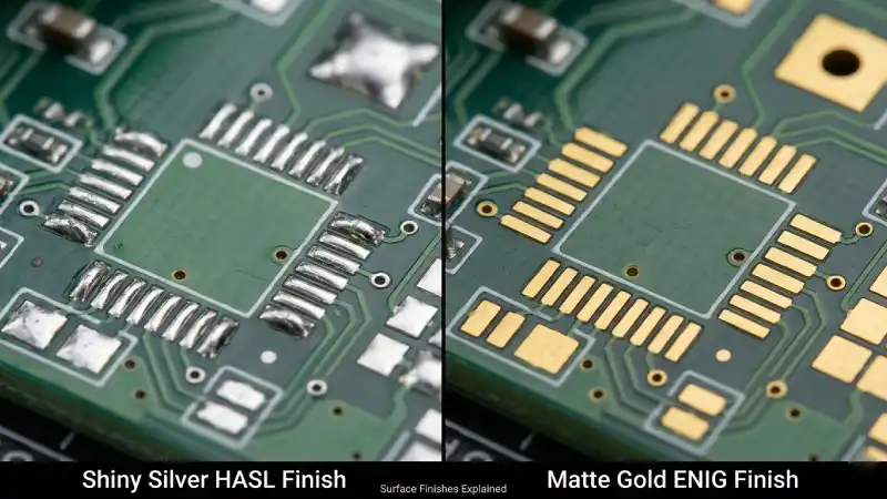
HASL — Hot Air Solder Levelling
The board is dipped in molten solder and then levelled with hot air knives. It produces a bright, solderable surface that is very forgiving for hand soldering.
- Cost: lowest
- Shelf life: 12 months
- Surface flatness: slightly uneven — not ideal for fine-pitch ICs below 0.5 mm pitch
- Lead-free HASL is the RoHS-compliant variant; slightly harder to solder than leaded HASL
ENIG — Electroless Nickel Immersion Gold
A thin layer of nickel is deposited on the copper, then a thin layer of gold is deposited on the nickel. ENIG produces an extremely flat, gold-coloured surface ideal for fine-pitch SMD pads and edge connectors.
- Cost: higher (roughly 2× HASL)
- Shelf life: 12–18 months
- Surface flatness: excellent — required for BGA and 0.4 mm pitch QFN
- Appearance: premium gold look
OSP — Organic Solderability Preservative
A thin organic compound is chemically bonded to the copper surface, preventing oxidation until the board is assembled. OSP is environmentally friendly and gives a very flat pad.
- Cost: low (similar to HASL)
- Shelf life: 6–9 months (shorter than HASL or ENIG)
- Note: OSP is transparent — the board looks like bare copper pads, not silver or gold
Immersion Silver
A thin layer of silver is deposited on the copper. It provides a flat surface, good solderability and better electrical performance than ENIG for RF applications.
- Cost: moderate
- Shelf life: 6–12 months; silver tarnishes if exposed to sulphur compounds
- Best for: RF designs and high-frequency PCBs where gold's slightly lower conductivity matters
What Does PCB LAB Use?
For student and maker orders, PCB LAB uses HASL (Lead-Free) as the standard surface finish. It offers the best balance of cost, solderability and shelf life for prototype quantities. If you need ENIG (for fine-pitch or gold fingers), contact us when placing your order.
For a first PCB: green solder mask + white silkscreen + HASL lead-free. This combination is cheap, widely compatible and perfectly suited for learning.
Order your board with the right finish.
5 boards — ₹450 total (₹150 setup + ₹300)
10 boards — ₹750 total (₹150 setup + ₹600) | Max 2 orders / month
Get a Quote →