Designing your first PCB can feel daunting — there are software tools to learn, design rules to follow and a whole new vocabulary to absorb. This guide strips it all back to the essentials so you can go from a blank canvas to a manufactured board without getting lost along the way.
Step 1: Draw Your Schematic
Every PCB starts with a schematic — a logical diagram showing how components connect to each other. Think of it as the blueprint before the physical layout. At this stage you are not concerned with where parts sit on the board; you are only defining what connects to what.
Free tools like KiCad and EasyEDA come with large component libraries so you can find most standard parts (resistors, capacitors, ICs, connectors) ready to place. Take your time here — a mistake in the schematic will carry through to the layout.
Step 2: Assign Footprints
A footprint is the physical pattern of copper pads on the PCB that corresponds to a component's physical package. A 100 Ω resistor schematic symbol can be a tiny 0402 SMD footprint or a through-hole axial footprint — you need to choose the one that matches the actual part you plan to solder.
Pro tip: Always cross-check the component datasheet for the recommended land pattern. Manufacturer footprints are the most reliable starting point.
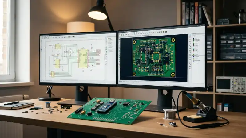
Step 3: Layout the Board
Once your schematic is complete and footprints are assigned, you import the netlist into the PCB layout editor. You will see all your components in a pile connected by thin "ratsnest" lines showing which pads need to be connected — your job is to arrange the parts and route those connections as copper tracks.
Layout best practices for beginners
- Keep the board outline (edge cuts) as compact as possible to reduce cost.
- Place decoupling capacitors as close as possible to IC power pins.
- Run power and ground traces wider than signal traces (1.5–2× at minimum).
- Avoid 90-degree trace bends — use 45-degree angles instead.
- On 2-layer (or higher) boards, add a solid ground plane on the bottom copper layer.
Step 4: Run Design Rule Checks (DRC)
Before generating manufacturing files, always run the DRC tool in your EDA software. It checks your layout against a set of rules (minimum trace width, clearance between conductors, drill sizes, etc.) and flags anything that could cause a manufacturing issue. Fix every error before moving on.
Step 5: Generate Gerber Files
Gerbers are the universal language between EDA software and PCB manufacturers. You will typically export:
- Top Copper (F.Cu)
- Bottom Copper (B.Cu)
- Top Solder Mask (F.Mask)
- Bottom Solder Mask (B.Mask)
- Top Silkscreen (F.Silkscreen)
- Board Outline (Edge.Cuts)
- Drill File (Excellon format)
Zip these files together and upload them to the PCB LAB quotation page.
Ready to Manufacture?
If you're a student or maker, PCB LAB offers subsidised single-sided boards — straightforward and affordable, ideal for getting your first prototype in hand. 5 boards for ₹450 total (₹150 setup + ₹300), or 10 boards for ₹750 (₹150 setup + ₹600). Upload your Gerbers, confirm the preview and place your order.
Student & Maker Offer
5 boards — ₹450 total (₹150 setup + ₹300)
10 boards — ₹750 total (₹150 setup + ₹600) | Max 2 orders / month
Get a Quote →