KiCad 8 is the most capable free PCB design tool available today. This tutorial takes you from a blank screen to a zip file ready to upload to PCB LAB — covering every step in the workflow without skipping anything a beginner might stumble on. Expect to spend 2–3 hours on your first board; the second one will take half the time.
Step 1: Install KiCad 8
Download KiCad 8 from the official website (kicad.org). It is available for Windows, macOS and Linux. During installation, include the default symbol libraries and default footprint libraries — these are large downloads (~2 GB) but essential. The 3D model library is optional; install it if disk space allows.
Step 2: Create a New Project
- Open KiCad 8. In the Project Manager, click File → New Project.
- Create a dedicated folder for the project (e.g.,
my-first-pcb/). Never store KiCad projects in shared or synced folders while editing — it can corrupt files. - KiCad creates two files:
project.kicad_sch(schematic) andproject.kicad_pcb(board layout).
Step 3: Draw the Schematic
Double-click the schematic file to open the Schematic Editor.
- Press A to open the symbol chooser. Search for components by name (e.g., "ATmega328", "LM7805", "LED").
- Place components on the canvas. Press W to draw wires between pins.
- Add power symbols (press A → search "VCC" and "GND") to all power and ground pins — do not leave pins unconnected.
- Use net labels (press L) to connect distant nets without drawing a wire across the whole schematic.
- Add a PWR_FLAG symbol to each power net to suppress ERC warnings about floating power pins.
When the schematic is complete, run Tools → Electrical Rules Checker (ERC) and resolve every error before proceeding.
Step 4: Assign Footprints
In the Schematic Editor, open Tools → Assign Footprints. For each symbol, select the physical footprint that matches the component you plan to use:
- Resistors / capacitors: choose 0603 or 0805 for beginner hand-soldering.
- ICs: match the exact package (SOIC-8, DIP-14, QFN-32, etc.) to the datasheet.
- Connectors: match the pin pitch and row count to your physical header.
Use the 3D viewer (View → 3D Viewer in the Schematic Editor) to visually confirm footprints look correct before moving on.
Step 5: Open the PCB Editor and Import Netlist
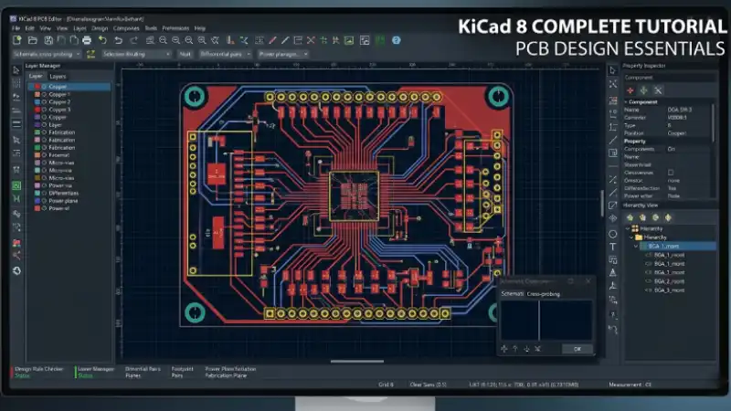
From the Schematic Editor, click Tools → Update PCB from Schematic (or press F8). All your components appear in a pile in the PCB editor connected by thin "ratsnest" lines. These lines show which pads need to connect — your job is to route them as copper tracks.
Step 6: Set the Board Outline
Select the Edge.Cuts layer. Draw a closed rectangle (or shape) defining your board size. Use Place → Line or the shortcut R for a rectangle. Common sizes for student projects: 50×50 mm or 100×80 mm.
Step 7: Set Design Rules
Go to File → Board Setup → Design Rules → Constraints and set:
- Minimum clearance: 0.2 mm
- Minimum track width: 0.2 mm
- Minimum via drill: 0.3 mm
- Minimum via annular ring: 0.15 mm
These match PCB LAB's manufacturing capabilities.
Step 8: Place Components
Drag components out of the pile and arrange them logically on the board. Good placement rules:
- Group components by function (power section, microcontroller section, connectors).
- Place decoupling capacitors immediately adjacent to their IC's power pins.
- Put connectors on the board edges for easy cable access.
- Rotate components so their connections flow in one direction — this minimises crossing ratsnest lines.
Step 9: Route Traces
Press X to activate the interactive router. Click a pad, route the trace to its destination and click to complete. The router automatically avoids obstacles and uses 45-degree bends.
- Route power traces first — thicker (0.5–1 mm) and they constrain the signal routing.
- Use vias to switch layers when traces cross. Press V while routing to place a via and flip to the other copper layer.
- Add a ground copper pour last: press Z, select B.Cu, assign GND net, draw the zone over the board, and press B to fill.
Step 10: Run DRC
Go to Inspect → Design Rules Checker and click Run DRC. Fix every error. Common errors and fixes:
- Clearance violation — move the offending trace or reduce its width slightly.
- Unconnected items — a ratsnest line is still there; finish routing that connection.
- Footprint outside courtyard — components are overlapping; space them further apart.
Step 11: Export Gerbers for PCB LAB
- Go to File → Plot.
- Set format to Gerber. Output directory: a subfolder called
gerbers/. - Enable layers: F.Cu, B.Cu, F.Mask, B.Mask, F.Silkscreen, B.Silkscreen, Edge.Cuts.
- Check Use Protel filename extensions for compatibility.
- Click Plot, then click Generate Drill Files (Excellon format, mm).
- Zip the
gerbers/folder and upload to PCB LAB.
Before uploading, open the zip in a Gerber viewer (or use PCB LAB's built-in preview) and confirm every layer looks correct. See our Gerber verification guide for the full checklist.
Gerbers ready? Upload them to PCB LAB.
5 boards — ₹450 total (₹150 setup + ₹300)
10 boards — ₹750 total (₹150 setup + ₹600) | Max 2 orders / month
Upload Gerbers →