When you open a new PCB project the software asks a question that surprises many beginners: how many layers do you want? The answer shapes everything — routing room, signal quality, manufacturing cost and turnaround time. This article breaks down the three most common layer counts and shows you how to pick the right one for your next design.
What Is a "Layer" in a PCB?
A PCB layer is a sheet of copper laminated inside (or onto the outside of) the board's FR-4 fibreglass substrate. Every layer can carry traces, pours and pads. The more layers you have, the more routing space you get — but also the higher the fabrication cost and complexity.
Layers always come in even numbers: 2, 4, 6, 8… The board must be symmetric around its centre to prevent warping during the lamination process.
2-Layer PCBs: The Sweet Spot for Most Makers
A 2-layer board has copper on the top and bottom. It is the most common choice for hobbyist and student projects and covers the vast majority of designs you are likely to build — microcontroller boards, sensor breakouts, motor drivers and power supplies.
Pros
- Cheapest to manufacture — PCB LAB's student price starts at ₹450 for 5 boards.
- Short lead times; widely supported by every fab.
- Simpler design rules to follow.
Cons
- Routing space is limited — dense designs can be tricky to complete without vias.
- No dedicated power or ground plane, so power delivery and EMI can suffer.
- High-frequency signals (above ~100 MHz) are harder to control.
Rule of thumb: if your design runs at 3.3 V or 5 V, clocks below 50 MHz and fits on a board smaller than 100×100 mm, a 2-layer PCB will almost certainly do the job.
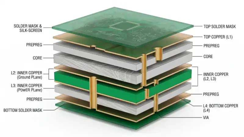
4-Layer PCBs: The Professional Step Up
A 4-layer board adds two internal copper layers between the outer surfaces. The standard industrial stackup is:
- Layer 1 (Top) — signal routing and components
- Layer 2 — solid ground plane (GND)
- Layer 3 — power plane (VCC / 3.3 V / etc.)
- Layer 4 (Bottom) — signal routing
The inner ground plane dramatically reduces electromagnetic interference (EMI) because every signal trace on the outer layers has a nearby reference plane beneath it. The power plane eliminates the need to route wide power traces across the board — power simply "floods" that layer.
When to choose 4 layers
- Your design includes a microprocessor running above 100 MHz.
- You have multiple supply voltages that would clutter a 2-layer layout.
- You need controlled impedance traces (USB, HDMI, LVDS, RF).
- BGA or fine-pitch QFN components make 2-layer routing impractical.
6-Layer PCBs: High-Speed and RF Designs
Six-layer boards are used in designs where signal integrity is critical — think Gigabit Ethernet, DDR memory interfaces or wireless RF front-ends. A typical 6-layer stackup looks like this:
- Signal (top)
- Ground plane
- Signal (inner)
- Signal (inner)
- Power plane
- Signal (bottom)
The two ground planes sandwiching the inner signal layers act as a Faraday cage, shielding high-speed traces from each other and from the outside world.
Cost Comparison at PCB LAB
As a rough guide, moving from 2 to 4 layers approximately doubles the board price, and 6 layers roughly doubles it again versus 4. For student and maker projects, a 2-layer design is almost always the most cost-effective starting point. Graduate to 4 layers only when the design genuinely demands it.
Quick Decision Guide
- Simple microcontroller / sensor board → 2 layers
- Raspberry Pi carrier / USB 2.0 / CAN bus → 2 or 4 layers
- ESP32 / STM32 with RF, DDR or USB 3.0 → 4 layers
- GHz-range RF, FPGA with DDR3, PCIe → 6+ layers
Ready to order your 2-layer board?
5 boards — ₹450 total (₹150 setup + ₹300)
10 boards — ₹750 total (₹150 setup + ₹600) | Max 2 orders / month
Get a Quote →