There comes a point in every maker's journey where a 2-layer board stops being enough — the routing is too congested, the power delivery is noisy or the RF performance is unpredictable. A 4-layer board solves all three problems simultaneously. This guide walks you through the stackup, the design decisions, and the practical steps in KiCad.
When to Move to 4 Layers
Upgrade from 2 to 4 layers when one or more of these conditions apply:
- You cannot complete routing without excessive layer jumps or impossible clearances.
- Your design has more than two supply voltages and routing power traces is messy.
- You are working with USB 3.0, Gigabit Ethernet, DDR memory or any high-speed interface.
- EMI compliance testing is required and a solid ground plane is essential.
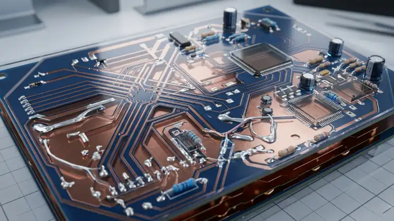
- You are placing BGA or fine-pitch QFN components that need breakout vias beneath them.
The Standard 4-Layer Stackup
The industry default for a 4-layer board is:
- Layer 1 — Top (Signal): Component placement, primary signal routing, high-density traces.
- Layer 2 — GND Plane: A solid, unbroken copper pour tied to GND. This is the most important layer in the stackup.
- Layer 3 — PWR Plane: One or more power voltages poured here. Can be split into zones for different rails (3.3 V, 5 V, 1.8 V, etc.).
- Layer 4 — Bottom (Signal): Secondary signal routing, less-critical traces, spillover from top layer.
The GND plane (Layer 2) must be solid and unbroken. Every split or cut in the ground plane creates an impedance discontinuity that forces return currents to take longer paths — the root cause of most EMI problems.
Setting Up Layers in KiCad
In KiCad's Board Setup dialog:
- Go to File → Board Setup → Board Editor Layers.
- Set copper layers to 4.
- Name the inner layers: In1.Cu → GND, In2.Cu → PWR.
- Set stackup thickness — standard 1.6 mm 4-layer FR-4 uses: 0.035 / 0.2 / 1.065 / 0.2 / 0.035 (copper / prepreg / core / prepreg / copper).
Creating Power Planes
Power planes in KiCad are copper pours (zones) on the inner layers:
- Select the In1.Cu (GND) layer.
- Add a copper zone (shortcut: Z) covering the entire board outline.
- Assign the zone to the GND net. Set fill to Solid.
- Repeat for In2.Cu (PWR), assigning the primary supply voltage net.
- If you have multiple supply voltages, split In2.Cu into zones — each zone is a different net, separated by a 0.3 mm gap.
- Press B to fill all zones. Check that the planes look solid with no unexpected breaks.
Via Stitching for EMI Control
Even with a solid ground plane, high-frequency currents need a low-impedance return path from the bottom layer back to the GND plane. Sprinkle GND stitching vias across the board — especially around high-frequency components, oscillators and switching converters — to stitch Layer 4 to Layer 2 at multiple points.
KiCad's "Add Vias Array" tool makes this fast: select the GND net, set a grid spacing of 3–5 mm and place vias across empty areas of the board.
Signal Routing Guidelines for 4-Layer Boards
- Route the majority of signals on Layer 1 (Top) — it is directly above the GND plane, providing a clean reference for return currents.
- Use Layer 4 (Bottom) for spillover signals and traces that would create congestion on top.
- Avoid routing signals on the inner planes — these are reserved for GND and power.
- For differential pairs (USB, Ethernet), route both lines on the same layer without switching layers mid-trace.
- Keep via transitions to a minimum for high-speed signals — each via adds parasitic capacitance and inductance.
Decoupling on a 4-Layer Board
With dedicated power and ground planes, decoupling capacitors become even more effective — the planes themselves act as a distributed capacitor. Place 100 nF ceramics directly under each IC VCC pin (via to PWR plane, via to GND plane) and you have a very clean power delivery network.
Cost at PCB LAB
4-layer boards are priced higher than 2-layer due to additional lamination steps. Contact PCB LAB for a 4-layer quote — for small student quantities (5–10 boards) the premium is often modest and well worth the routing freedom and EMI improvement.
Ready to go 4-layer?
Contact PCB LAB for a custom 4-layer quote tailored to your project's dimensions and quantity.
Get a Quote →