Copper traces are wires — and like any wire, they have a resistance and a maximum current they can carry before heating up. Size a trace too thin and it becomes a fuse. Size it too wide and you waste routing space. This guide gives you the tools to get it right every time.
Why Trace Width Matters
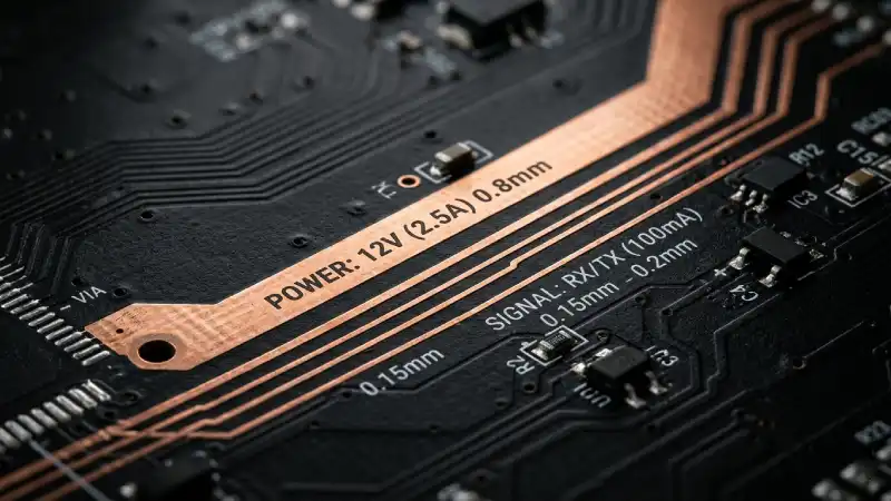
Current flowing through copper generates heat (P = I²R). If a trace is too narrow, it heats up, can oxidise the solder mask above it, and in extreme cases can open-circuit like a fuse. For signal traces carrying only a few milliamps, this is never an issue — but for power lines supplying motors, LEDs or voltage regulators, trace width is a critical design parameter.
The IPC-2221 Standard
The electronics industry uses the IPC-2221 standard to relate trace width to current capacity. The simplified formula is:
I = k × ΔT0.44 × A0.725
Where I is current (A), k is 0.048 for internal layers and 0.048×1.5 for external layers, ΔT is the allowable temperature rise above ambient (°C), and A is the cross-sectional area of the trace (mils²). Most designers use an online calculator rather than computing this by hand.
Practical Quick-Reference Table
Based on IPC-2221, assuming 1 oz copper (35 µm) and 10°C temperature rise above ambient:
| Current | External trace width | Internal trace width |
|---|---|---|
| 0.3 A (signal, GPIO) | 0.15 mm (6 mil) | 0.2 mm (8 mil) |
| 0.5 A (LED strings) | 0.25 mm (10 mil) | 0.35 mm (14 mil) |
| 1 A (small motors, 3.3 V rail) | 0.5 mm (20 mil) | 0.7 mm (28 mil) |
| 2 A (USB-C PD, servo power) | 1.0 mm (40 mil) | 1.4 mm (56 mil) |
| 5 A (battery main line) | 2.5 mm (100 mil) | 3.5 mm (140 mil) |
PCB LAB minimum trace width: 0.15 mm (6 mil). Always stay at or above this limit — traces below it will not reliably survive the etching process.
Signal Traces vs Power Traces
For digital signal traces (SPI, I²C, UART, GPIO) that carry only a few milliamps, use 0.2 mm as a safe default. This is well above the fab minimum, easy to route around dense IC pads and still provides good yield.
For power rails, refer to the table above and add a 20% margin — traces run warmer in enclosed enclosures, so budget headroom keeps your board cool in real-world conditions.
The Ground Plane Shortcut
The best practice for PCB power distribution is to use a copper pour (flood fill) tied to GND rather than routing individual ground traces. A ground plane has essentially zero resistance, eliminates the trace-width question for return currents, and reduces EMI significantly. Use poured copper for GND and size your VCC traces correctly — this covers 90% of maker designs cleanly.
Online Calculators
Rather than doing the IPC-2221 math manually, use a dedicated calculator. Search for "PCB trace width calculator IPC-2221" — several free browser tools exist. Enter your current, copper weight (1 oz is standard) and allowed temperature rise, and read off the required width directly.
Traces sized? Time to build.
5 boards — ₹450 total (₹150 setup + ₹300)
10 boards — ₹750 total (₹150 setup + ₹600) | Max 2 orders / month
Get a Quote →